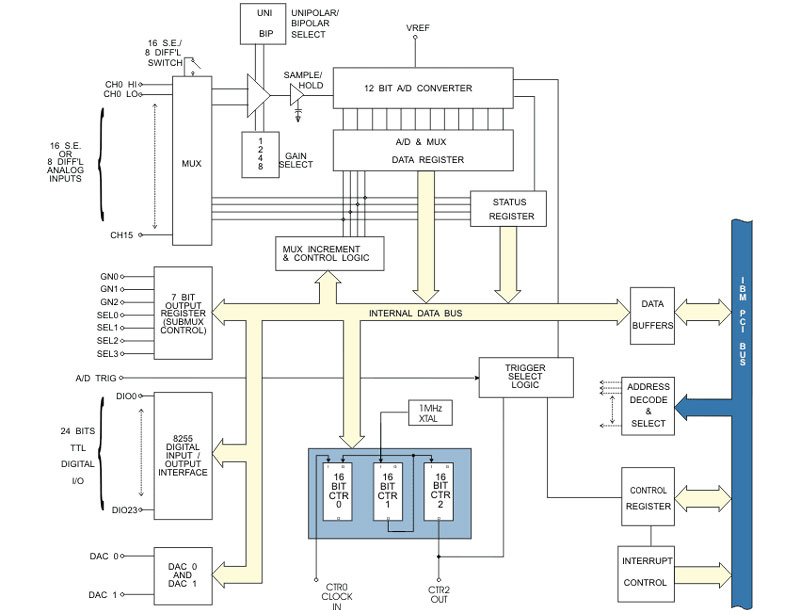
● PCI Bus
● Type: Successive approximation.
● Resolution:12-bit
● Ranges:
- Unipolar Voltage: 10V, 5V, and offset ranges 1.25V to 3.75V and 1.25V to 6.25V
- Bipolar Voltage: ±10V, ±5V, ±2.5V, and ±1.25V
- Current: 4-20 mA. (When this range is selected amplifier gain and offset are automatically adjusted so that full 12-bit resolution is achieved.)
● Conversion Time: 8 μsec max., 5.7 μsec typical.
● Integral Linearity Error: ±0.45 LSB maximum.
● Differential Non-Linearity: No missing codes.
● Overall Accuracy: ±0.25%
● Sample and Hold Acquisition Time: 2 µsec for a full-scale step input
● Aperture Delay: 40 nsec typical
● Throughput: Up to 100 Ksamples per second
● Zero Drift: ±2 ppm/°C typical
● Full Scale Drift: ±5 ppm/°C typical
● Acquisition Time: 1 microsecond to 0.01% typical for full scale step function input.
● Aperture Uncertainty: 0.3 nanosecond typical.
● Voltage: +10 VDC ±0.2 VDC
● Temp. Coefficient: ±30 ppm/°C.
● Load Drive: 200mA maximum.
● Four-Bit Digital I/O:
- Input Voltage: Logic High is 2.0V min, Logic Low is 0.8V max
- Output Drive: 350 mA (sink only) each output with 20 mSec pulse width and a 30% duty cycle
● Seven-Bit Digital Output: Drives 25 mA maximum
● Type: 82C54-2 programmable interval timer.
● Counters: Three 16-bit down counters, two permanently concatenated with 1MHz clock as programmable timer.
● Output Drive: 2.2mA at 0.45V (5 LSTTL loads).
● Input Gate: TTL/DTL/CMOS compatible.
● Clock Frequency: Internal: 1 MHz;External: DC to 10 MHz
● Active Count Edge: Negative edge.
● Min Clock Pulse Width: 30nS high/50nS low.
● Timer Range: 2.5 MHz to <1 pulse/hr.
● Operating Temp: 0 °C. to 50 °C.
● Storage Temp: -20 °C. to +70 °C.
● Humidity: 0 to 90% RH, non-condensing.
● Power Required: +5VDC: 600 mA typical.
- +5 VDC @ 900 mA typical
- +12 VDC @ 125 mA typical
- – 12 VDC @ 125 mA typical
● This product is designed to be in full compliance with CE requirements.